StackUp 3D / USB-C contact study
Give every
contact room.
A connector can fit on the outside while the space between its contacts still needs attention. Follow one selected gap, see what consumes its clearance, and test a more focused positioning requirement.
44 seconds / Silent film with on-screen explanations
Download illustrated studyThe result
One positioning change.
40 µm more clearance.
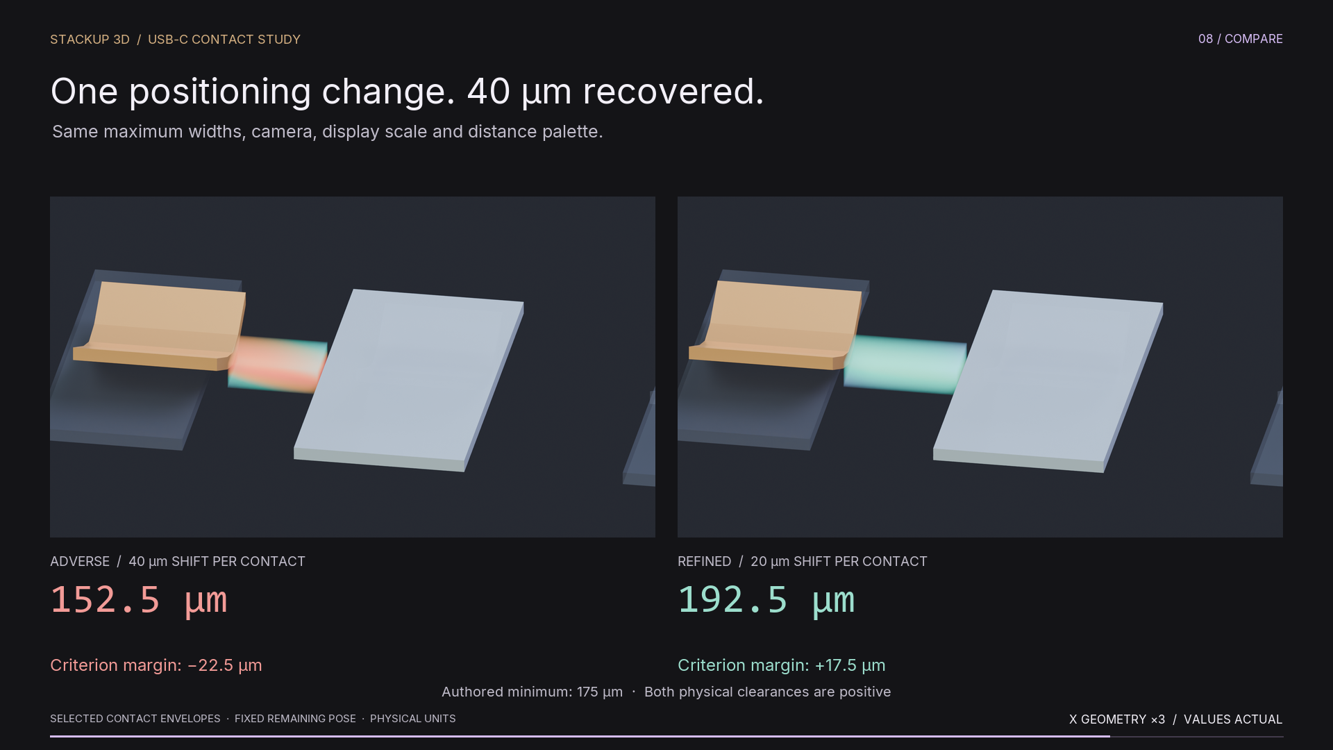
The adverse and refined cases use identical maximum contact widths. Reducing the opposing position shifts increases the selected physical gap from 152.5 to 192.5 µm.
Selected nominal widths and aligned contact centers.
Maximum contact widths; opposing 40 µm shifts per contact.
The same maximum widths; opposing 20 µm shifts per contact.
The example target is 175 µm minimum clearance, chosen for this study. All three gaps remain positive; the adverse case is 22.5 µm below that target, and the refined case is 17.5 µm above it.
01 / Define the relationship
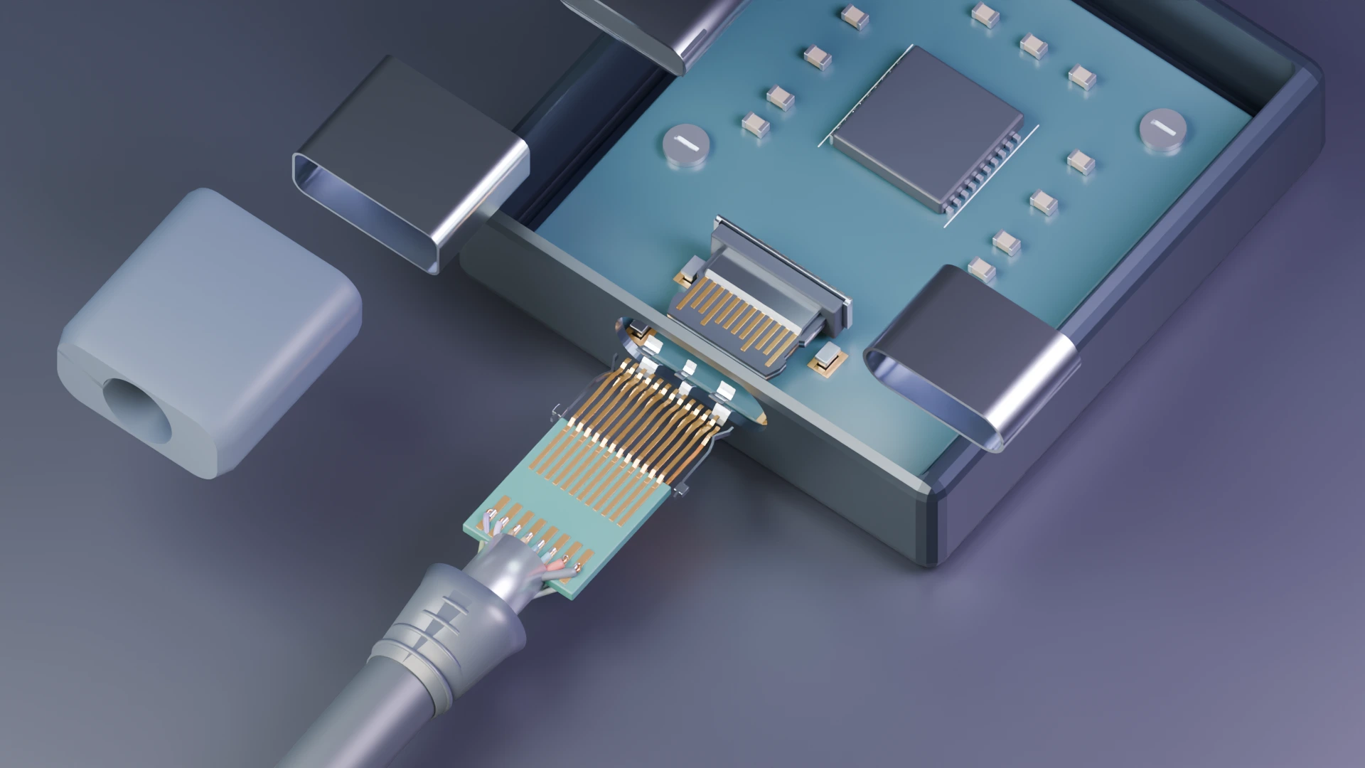
From the cable
to the contact array.
The selected measurement runs from plug contact P_A6 to neighboring receptacle contact R_A7. The exploded view reveals both arrays; the analysis uses a defined inspection pose with aligned datum frames.
02 / Review the evidence
See the geometry.
Check the gap.
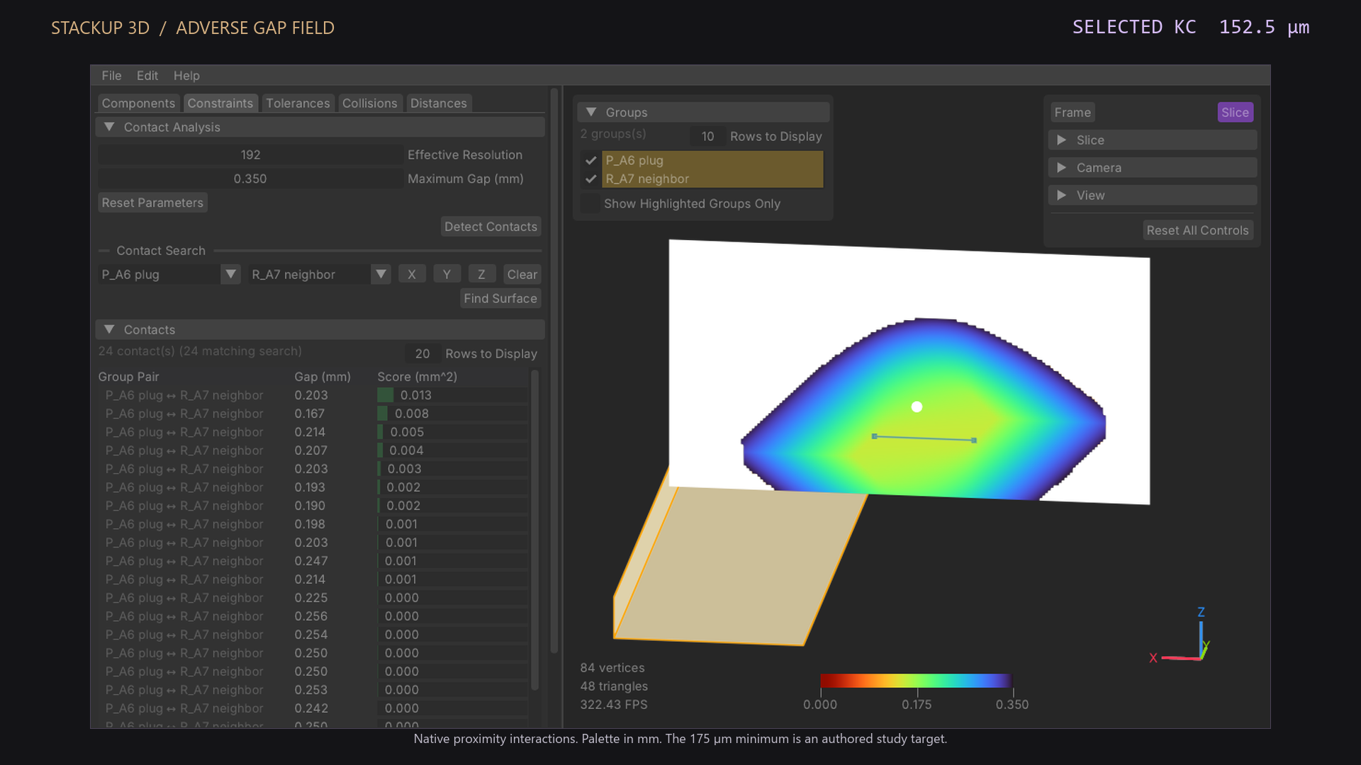
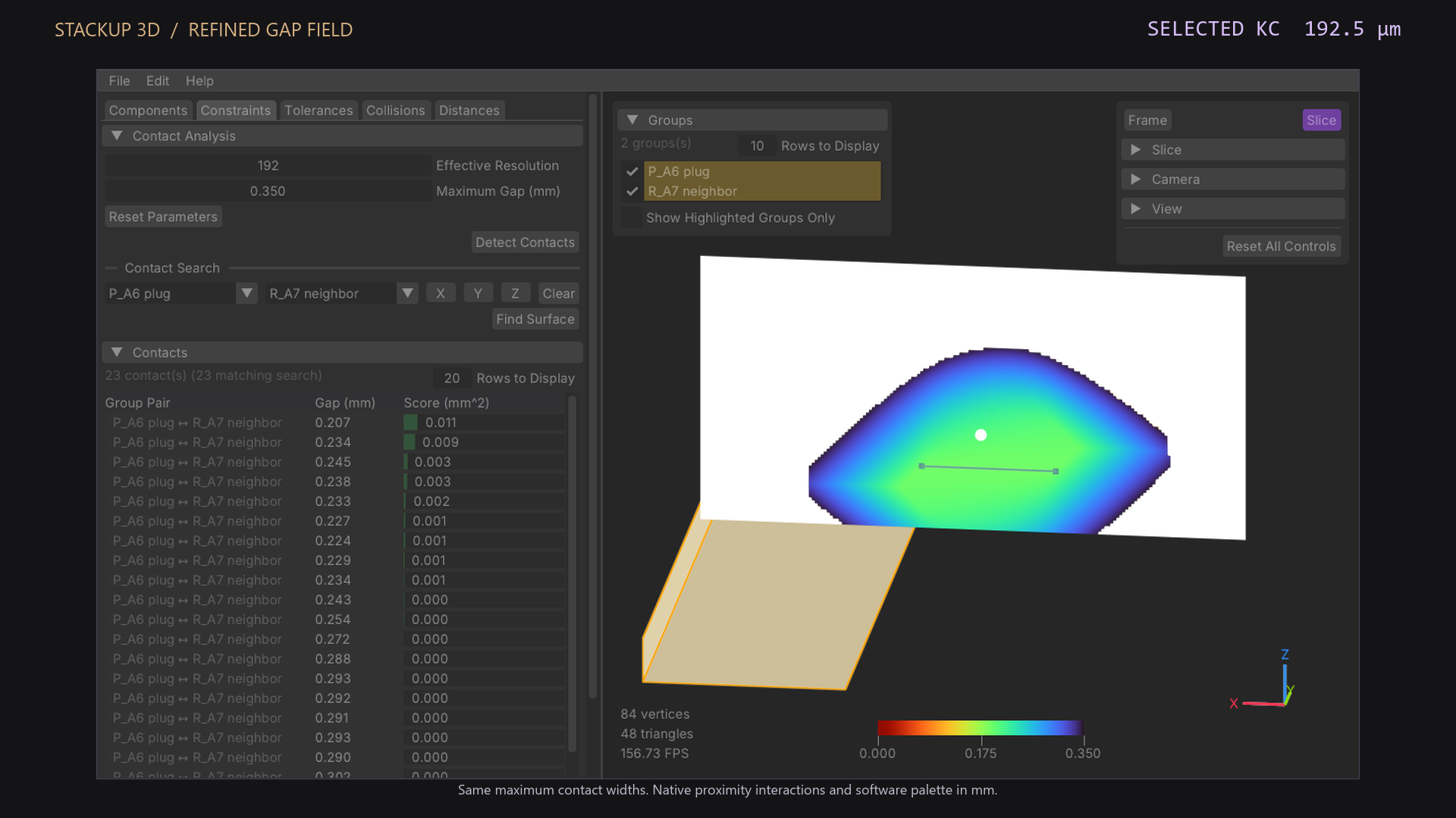
These are actual StackUp 3D captures of the evaluated geometric states. Native point-distance results agree with independent CAD distance checks for the selected contact envelopes.
Measurement and presentation notes
This is an illustrative geometric study of selected contact envelopes, with aligned datum frames and the remaining pose fixed. The 175 µm target and tighter positioning requirement are authored study choices, rather than USB-C certification limits. Electrical behavior, contact force and process yield are outside its scope.
The macro renders enlarge geometry 3× along X to make the gap visible; the displayed measurements retain physical units. Native application views use physical geometry. Software field legends are in millimetres and use a different palette from the rendered views.
Native distance labels round to 0.001 mm. A displayed zero sigma describes the imposed geometric state, not zero manufacturing variation. Software inserts are held captures, and dissolves between evaluated fields are editorial transitions.